1 北京航空航天大学物理学院,北京 100191
2 澳大利亚国立大学物理学院电子材料工程研究室,澳大利亚堪培拉 2601
超分辨荧光成像技术因其能够突破光学衍射极限的限制,为生命科学研究带来全新的观察尺度而获得了诺贝尔化学奖。但是,传统的超分辨荧光显微镜需要极为复杂的光学系统来突破衍射极限,通常伴随着明显的光毒性和低时间分辨率,昂贵的造价以及日益复杂的操作限制了其在生物医学领域中的推广应用。因此,全球各大研究团队都在积极寻求具有近红外、高亮度和抗光漂白的替代荧光探针,并通过改善成像装置与算法,进一步拓展超分辨显微技术的应用范围。稀土元素纳米材料由于其独特而优异的物理化学特性,如显著的反斯托克斯光谱位移、无背景噪声、抗光漂白、光稳定性、低毒性和高成像穿透能力等,持续受到化学、物理学和材料学领域的广泛关注,是近期兴起的一种稳定性优异的无机荧光探针。本文首先简要介绍了上转换纳米颗粒的发光机制,然后讨论了纳米结构材料中实现光子上转换的主要限制。此外还介绍了镧系元素掺杂上转换纳米粒子在超分辨生物成像、分子检测等领域的应用,以及介绍了包括降低激光功率要求和耦合技术难度、提高激光直扫成像分辨率与速度、提高多路复用成像效率等应用技术优势。最后重点介绍了颗粒合成方面的主要挑战、可行的改进措施以及对未来发展的展望,为稀土纳米材料在生命科学成像领域的推广应用提供有力的理论基础与技术支撑。
荧光显微 超分辨成像 上转换纳米颗粒 镧系离子掺杂 激光与光电子学进展
2024, 61(6): 0618018
Author Affiliations
Abstract
1 School of Physics, State Key Laboratory of Crystal Materials, Shandong University, Jinan 250100, China
2 Collaborative Innovation Center of Light Manipulations and Applications, Shandong Normal University, Jinan 250358, China
3 Key Laboratory of Materials for High-Power Laser, Shanghai Institute of Optics and Fine Mechanics, Chinese Academy of Sciences, Shanghai 201800, China
4 Department of Physics, Center for Ion Beam Application and Center for Electron Microscopy, Wuhan University, Wuhan 430072, China
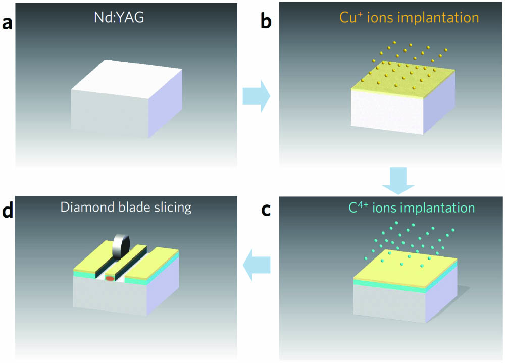
Copper (Cu) nanoparticles (NPs) are synthesized under the near-surface region of the (Nd:YAG) crystal by direct ions implantation. Subsequently, the monolithic ridge waveguide with embedded Cu NPs is fabricated by ions irradiation and diamond saw dicing. The nonlinear optical response of the sample is investigated by the Z-scan technique, and pronounced saturable absorption is observed at the 1030 nm femtosecond laser. Based on the obvious saturable absorption of Cu NPs embedded Nd:YAG crystal, 1 μm monolithic mode-locked pulsed waveguide laser is implemented by evanescent field interaction between NPs and waveguide modes, reaching the pulse duration of 24.8 ps and repetition rate of 7.8 GHz. The work combines waveguides with NPs, achieving pulsed laser devices based on monolithic waveguide chips.
waveguide lasers nanoparticles localized surface plasmon resonance saturable absorption Chinese Optics Letters
2021, 19(2): 021301
1 湖北工业大学机械工程学院, 湖北 武汉 430068
2 现代制造与质量工程湖北省重点实验室, 湖北 武汉 430068
提出了一种双频曲线拟合的亚像素中心提取方法。首先采用二次阈值法自动分割光条区域,利用灰度重心法获取光条纹中心初始位置,然后用移动直线拟合初始位置得到光条曲线的局部法线,最后在法线方向上进行双频曲线拟合,得到光条纹中心的亚像素坐标。实验结果表明,该方法能消除部分高频噪声的影响。相比Steger法,该方法提取的条纹中心均方根误差小于0.1 pixel,速度约是其26倍,可适用于多种材质表面光条纹中心的提取,为工业应用中的激光条纹中心提取提供参考。
机器视觉 条纹中心提取 双频曲线拟合 线结构光 激光与光电子学进展
2020, 57(14): 141502
山东大学物理学院, 晶体材料国家重点实验室, 山东 济南 250100
飞秒激光直写是一种高效灵活的三维精密材料加工技术,在许多领域得到了广泛的应用。光波导是集成光子学器件的一种基本结构,能够将光场限制在微小的通道内进行无衍射的传输。激光晶体是全固态激光器的常用增益介质,利用飞秒激光直写技术在激光晶体上构建光波导结构,并保持晶体的原有属性,从而可以制备低成本、高效率的波导激光器件。从飞秒激光诱导晶体产生的两类结构改性(折射率改变)出发,综述了飞秒激光直写激光晶体光波导的种类、特性以及应用,并对相关领域的应用前景进行了展望。
激光光学 飞秒激光直写 激光晶体 光波导 波导激光 分束器 激光与光电子学进展
2020, 57(11): 111415
山东大学物理学院,晶体材料国家重点实验室, 山东 济南 250100
光波导是集成光学中的基本元件之一,构建于光波导结构上的波导激光器是一种微型激光源,近年来受到较多研究人员的关注,并有望在未来光子学系统中发挥重要的作用。激光晶体是固态激光器的主要增益介质之一。本文综述了基于激光晶体的固态波导激光器的最新研究进展,包括连续波波导激光器和脉冲波导激光器(调Q或锁模),其工作波长涵盖了从可见光到中红外的各个波段;还对波导激光研究的未来发展方向进行了展望。
激光器 光波导 波导激光 激光晶体 连续波激光 调Q激光 锁模激光
Author Affiliations
Abstract
1 School of Physics, State Key Laboratory of Crystal Materials, Shandong University, Jinan 250100, China
2 State Key Laboratory of Crystal Materials and Institute of Crystal Materials, Shandong University, Jinan 250100, China
Graphene and other extraordinary two-dimensional materials together with recent advances in optical modulators have set the foundations for the widespread applications of next-generation optoelectronic devices. In this work, we report on the high-performance fundamentally mode-locked waveguide laser modulated by chemical-vapor-deposition-grown WSe2 as a saturable absorber. By incorporating a WSe2 sample into a monolithic Nd:YVO4 waveguide platform, 6.526 GHz picosecond pulsed laser generation has been achieved at the wavelength of 1 μm with pulse duration of 47 ps.
160.4236 Nanomaterials 140.4050 Mode-locked lasers 140.3540 Lasers, Q-switched Chinese Optics Letters
2019, 17(2): 020013
Author Affiliations
Abstract
1 School of Physics, State Key Laboratory of Crystal Materials, Shandong University, Jinan 250100, China
2 Key Laboratory of Materials for High-Power Laser, Shanghai Institute of Optics and Fine Mechanics, Chinese Academy of Sciences, Shanghai 201800, China
3 Laser Microprocessing Group, Facultad Ciencias, Universidad de Salamanca, Salamanca 37008, Spain
4 School of Chemistry and Chemical Engineering, Shandong University, Jinan 250100, China
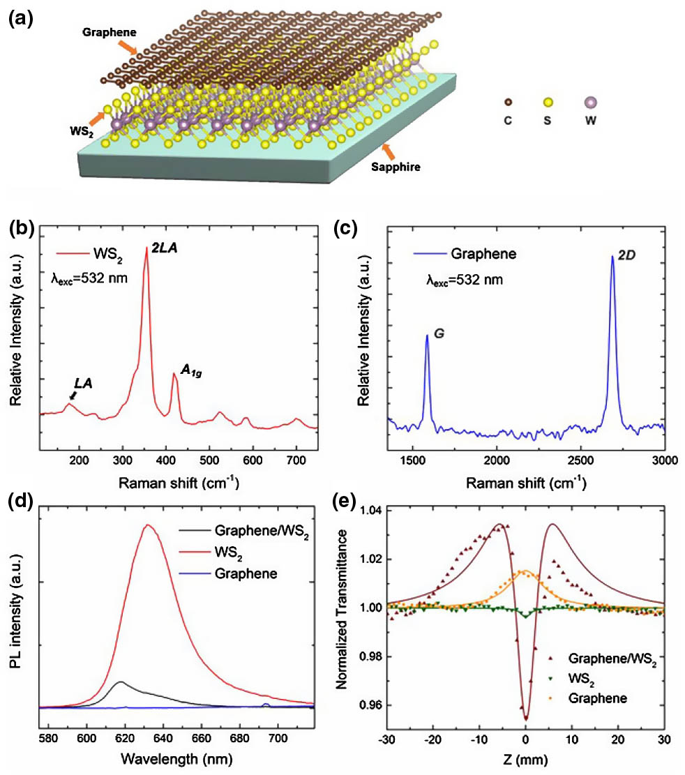
We report on the operation of passively Q-switched waveguide lasers at 1 μm wavelength based on a graphene/WS2 heterostructure as a saturable absorber (SA). The gain medium is a crystalline Nd:YVO4 cladding waveguide produced by femtosecond laser writing. The nanosecond waveguide laser operation at 1064 nm has been realized with the maximum average output power of 275 mW and slope efficiency of 37%. In comparison with the systems based on single WS2 or graphene SA, the lasing Q-switched by a graphene/WS2 heterostructure SA possesses advantages of a higher pulse energy and enhanced slope efficiency, indicating the promising applications of van der Waals heterostructures for ultrafast photonic devices.
(230.7370) Waveguides (140.3540) Lasers Q-switched (130.0130) Integrated optics (160.4236) Nanomaterials. Photonics Research
2017, 5(5): 05000406


